高価で複雑なディスクリート相互接続ケーブルは、設計の信頼性を低下させ、設計コストと全体の設計サイズを増大させる可能性があります。 実際には、個別の相互接続ケーブルは不利な設計です。 電子製品の販売者にとっては、電子製品の小型化のトレンドに反するものであり、PCBA メーカーにとっては信頼性の低い設計です。 プロジェクト リーダーにとって、ディスクリート相互接続ケーブルは高価であるだけでなく、より複雑です。 幸いなことに、FS Technology のリジッド フレックス PCBA は完全な代替品となります。
FS Technology は、このリジッド フレックス PCBA の製造を専門としています。この PCBA は、柔軟性と信頼性を考慮して設計されており、電子プロジェクトに費用対効果が高く便利なソリューションを提供します。 ディスクリート インターコネクトでは導体の向きが異なりますが、フレックス PCBA ではすべての導体が特定の方向に固定されています。 信頼性と柔軟性を備えた PCBA トレースの正確なモデリングとより予測可能な設計。
また、FPCの部分にはゴールドフィンガーコンタクトを採用するFS Technologyにより、FPCのエッジをコネクタのオス部分として使用することができ、高密度設計に対応できます。 今日、電子製品ユーザーのニーズを満たすために、このリジッド フレックス PCB は、ほとんどすべての従来のディスクリート相互接続ソリューションに取って代わり、高度なモジュール設計を可能にします。
FS Technology のフレキシブル PCBA は、相互接続ソリューションを設計および製造するための効果的な方法を提供するだけでなく、回路基板の収容を強化し、ソリューションの焦点となります。リジッド フレックス PCB を使用すると、電子製品の体積を小さくすることができます。これは、従来の回路基板に匹敵するものではありません。コンポーネントをリジッド PCB に取り付ける代わりに、FS Technologies が製造したボードをすべての柔軟なソリューションに取り付けることができます。上記の利点に加えて、リジッド フレックス PCBA のリジッド部分は補強材として機能し、フレキシブル PCB では不可能な信頼性を電子プロジェクトに提供します。現在使用されているウェアラブル デバイス、デジタル カメラ、医療機器のほとんどは、FPC やリジッド PCBA だけでなく、リジッド フレックス PCB を使用しています。
FS Technology は、柔軟なリジッド PCB がすべての柔軟性ソリューションの中で最高のものであると考えています。 2 つのボード間の相互接続が組み込まれたフレックスリジッド設計が特徴です。 FS Technology によって製造されたリジッド フレックス PCBA をさまざまなソリューションで使用することで、設計者は 1 つの組み立てステップで 3D ソリューションに対応できます。従来の回路基板やディスクリート接続の代わりにリジッド フレックス PCBA を使用すると、機械的組み立ての組み立て時間を短縮できます。電子製品の販売者による PCB の需要が高まるにつれて、リジッド フレックス PCB があらゆる電子ソリューションの触媒であることが証明されています。
リジッドフレックス PCB は従来の PCB よりも優れていますが、設計プロセスは非常に似ています。ターンキー PCB メーカーとして、フレキシブル パーツを作成する際には、機械的品質に特別な注意を払う必要があります。フレキシブル PCB 設計の 2D レイアウトを作成する場合、3D モデリング ソフトウェアを使用してフレキシブル設計のモックアップを作成するか、設計のペーパー モックアップを作成するのが最適です。この方法は、設計がフレキシブル基板の機械的仕様を満たしているかどうかをテストするのに便利です。それに加えて、設計する PCB の曲げ半径は、フレックス PCB の許容範囲よりも小さくする必要はありません。
FS Technology では、リジッドフレックス PCB を設計する際に次の点に注意することをお勧めします。
フレックス回路の各層にスタガード トレースを配置することで、基板の柔軟性を高めます。
リジッドフレックス PCB の製造ファイルを FS Technology に送信する前に、フレックス ボードが曲げ可能であり、ネストされたときに最高の密度になるなど、計画の実行可能ファイルを事前に検討してください。 PCBを曲げることで特定の寸法が達成できる場合、通常、最初の設計では曲げませんが、組み立て段階で曲げます。最後に、あなたが設計するいくつかのリジッド フレックス PCBA は、フレキシブル PCB よりも高価であることを知っていただければ幸いです。プロジェクトのニーズに合わせて使用するレイヤーの数を減らすようにしてください。販売する電子機器の収益性が高くなります。柔軟で堅固なソリューションは、設計に非常に多くの層数の要件がある場合にのみ考慮する必要があります。
最後に、フレックス PCB の充填はリジッド PCB の充填と非常に似ています。フレキシブル PCB の組み立てを行うときは、次のヒントを考慮してください。
フレックス PCB を 1 時間焼いた後、それらを埋めて吸収した水分を取り除きます。
フレックス PCB を固い表面に固定して、デバイスにはんだ付けしたときに寸法安定性を確保します。
デバイスをフレックス PCB に手作業ではんだ付けする場合は、フレックス PCB の部品の過熱を避けるために、はんだを多用する固定具を飛ばしてください。
結論として、リジッドフレックス PCB は、電子機器製造プロセスのコストと複雑さを大幅に削減できます。リジッド フレックス PCBA は、柔軟なフォーム ファクタで PCB の再現性と信頼性を提供する、従来のディスクリート ルーティング ソリューションの優れた代替品です。さらに、リジッド フレックス PCBA は、組み立てコストを低く抑え、高い再現性と信頼性を維持しながら、非常に複雑な 3D 設計を作成する機会を提供します。要するに、リジッド フレックス ボードを使用すると、コストがかかりすぎたり、複雑すぎたり、単に製造が不可能な設計を扱うことができます。リジッド フレックス ボードを使用して、設計を次のレベルに引き上げます。
With the development of the electronics manufacturing industry, human beings improve the functions of electronic products through PCB boards. As the best one-stop PCB company in China, FS Tech believes that it is our responsibility to show the world our manufacturing capabilities, assembly capabilities and testing capabilities to do our part for the PCB industry. In order to facilitate the novice in the PCB industry, we will distinguish the blog website according to different types: printed circuit board materials 、PCB motors 、printed circuit board printing 、pcb soldering
When designers are designing Rigid PCBAs, hint layout is certainly considered one among their key tasks. Designers can without difficulty calculate the present day wearing potential of the Rigid PCBA board via the PCBA hint present day calculator. The cause why Rigid PCBA strains are of precise situation is that it immediately influences the present day potential. The IPC-2221 General Design Guidelines are a very good start line for without difficulty measuring the width of board conductors or “strains” with a programmed formula. Of course, its energy isn't always most effective to this, it is usually greater effective features, such as: the period of the hint, the entire resistance cost of the circuit board, the energy loss as a result of the hint resistance. Note : The Trace Calculator is an effective layout tool, however its consequences aren't genuine and want to be adjusted in step with the real software of the project. In the subsequent content, FS Technology will recognition at the creation of hint calculation formulation and symbols.
The minimal width and thickness of conductors at the completed FS Technology Rigid PCBA board want to be decided consistent with the present day sporting capability required with the aid of using the venture and the most allowable conductor temperature rise. For conductors on outer and internal layers of revealed boards, minimal conductor width and thickness. As proven below:


We can calculate the size of the cross-sectional area according to the formula provided by FS Technology
A = (I / (k * T RISE b )) 1/c
The formula for calculating the maximum current that a trace can carry is as follows:
W = A / (T * 1.378 [mils/oz/ft 2 ])
Explain :
A : Refers to the size of the cross-sectional area, the unit is mils²
T : Refers to the thickness of the FS Technology Rigid PCBA trace, the unit is oz/ft²
W : Refers to the trace width, the unit is mils
IMAX : Refers to the maximum current that the trace runs through, the unit is A
T RISE : Refers to the maximum desired temperature rise, the unit is °C
K, B, C : Refer to constant values. According to IPC-2221A standard, 6.2 (“Requirements for Conductive Materials”), their inner layer values are as follows : K = 0.048 B = 0.44 C = 0.725
The formula for calculating the total trace temperature of the circuit board is as follows:
TTEMP = TRISE + TAMB
Explain :
T TEMP : Refers to the temperature of the trace, the unit is °C
T RISE : Refers to the maximum desired temperature rise, the unit is °C
T AMB : Refers to the ambient temperature, the unit is °C
We outline the allowable temperature upward push of the conductor because the distinction among the important cost of the secure working temperature of the FS Technology Rigid PCBA laminate and the most temperature that the Rigid PCBA can withstand. For convection cooled PCBA assemblies, the thermal surroundings is the most ambient temperature at which the broadcast board may be used. For conduction-cooled PCBA assemblies in a convection surroundings, the temperature upward push is because of the strength dissipated through the conduction-cooled additives, and the temperature upward push via the broadcast board and/or warmth sink to the bloodless plate need to additionally be considered. For conduction cooled FS Technology Rigid PCBA assemblies in a vacuum surroundings, the thermal surroundings is the temperature upward push because of the dissipated strength of the additives and the temperature upward push via the FS Technology PCBA and/or warmth sink to the bloodless plate.
Convert the cross-sectional area from mils² to cm² before doing the calculation:
A’ = A * 2.54 * 2.54 * 10-6
Begin to calculate the resistance, the formula for the resistance calculation is as follows:
R = (ρ * L / A’) * (1 + α * (TTEMP – 25 °C))
Explain :
T : Refers to the thickness of the trace, the unit is mils²
W : Refers to the trace width, the unit is mils
R : Refers to the resistance value, the unit is Ω
ρ : Refers to the resistivity parameter, the resistivity parameter of copper is 1.7E-6 [Ω·cm]
L : Refers to the trace length, the unit is cm
α : Refers to the temperature coefficient of resistivity, copper has a temperature coefficient of resistivity of 3.9E-3 [1/°C]
T TEMP : Refers to the trace temperature, the unit is °C
The formula for calculating the voltage drop is as follows :
VDROP = I * R
Explain :
V DROP : Refers to the voltage drop, the unit is V
The formula for calculating FS Technology Rigid PCBA power consumption is as follows:
PLOSS = R * I2
Explain :
P LOSS : Refers to power loss, the unit is W
Example 1
Inputs W = 12 mil T = 5 mil TRISE = 30 °C TAMB = 25 °C L = 12 inch
Output Cross-section Area = 60.00 mils2 IMAX = 4.17 A
Additional output Trace Temperature = 55 °C Resistance = 0.150 Ω Voltage Drop = 0.626 V Power Dissipation = 2.608 W
Example 2
Inputs W = 10 mil T = 3 oz/ft2 TRISE = 20 °C TAMB = 18 °C L = 25 cm
Output Cross-section Area = 41.34 mils2 IMAX = 2.66 A
Additional output Trace Temperature = 38 °C Resistance = 0.167 Ω Voltage Drop = 0.444 V Power Dissipation = 1.182 W
With the development of the electronics manufacturing industry, human beings improve the functions of electronic products through PCB boards. As the best one-stop PCB company in China, FS Tech believes that it is our responsibility to show the world our manufacturing capabilities, assembly capabilities and testing capabilities to do our part for the PCB industry. In order to facilitate the novice in the PCB industry, we will distinguish the blog website according to different types: printed circuit board materials 、PCB motors 、printed circuit board printing 、pcb soldering
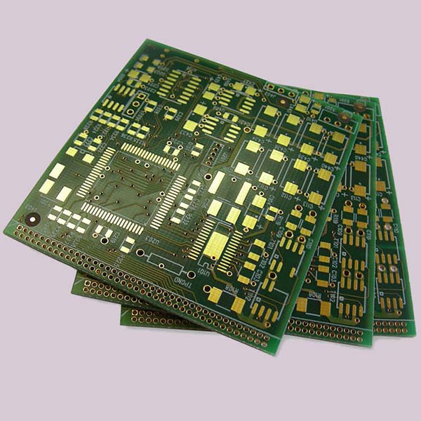
Almost all electronic devices have PCB boards, from electronic watches commonly used in the home, calculators, communication electronic devices, to military weapon systems, that is to say, as long as there are electronic components such as integrated circuits, in order to interconnect them, we must Use pcb. Let's follow the turnkey PCB assembly company FS Technology to see the classification and process flow of pcb equipment.

In the study of large electronic products, the most fundamental success factors are the design, documentation, fabrication and PCB assembly of the product's printed circuit boards. PCB design and manufacturing quality directly affect the quality and cost of the entire product, and even lead to the success or failure of business competition.
PCB manufacturing process: incoming plate→pickling→pump washing→city washing→four brushes with swing plate→high pressure infusion pump washing (20 Kg/cm 2 )→pump cleaning→city washing→suction→drying→drying→discharging.
For some companies that do not want to assemble PCBs and want to directly obtain products and start selling, the procurement and welding of PCB components is very troublesome. You can take a look at the FS Technology PCB component procurement capabilities. We can meet the needs of most customers.
On the insulating substrate, according to a predetermined design, a printed circuit, a printed element or a combination of two conductive patterns is made, which is called a printed circuit.
On the insulating substrate, electrical connection channels are provided for the components, and the conductive pattern of the device is called a printed circuit. It does not include printed components. Electronic components are assembled by a one-stop PCB assembly company after producing bare PCB boards.
The printed circuit board is called a PCB board, also called a PC board, and the assembled PCB board is called a PCBA board.
According to the degree of rigidity and flexibility of the substrate: rigid PCB board, flexible PCB board and rigid-flex PCB board.
According to the number of layers of the PCB: single-sided, double-sided and multi-layer printed boards.
The position of conductor pattern and substrate: flat printed board and curved PCB board.
More PC board terms and definitions can be found on the PCB org website or on the PCBA blog of one-stop PCB assembly company FS Technology.
The use of printed boards in electronic equipment avoids errors in manual wiring due to the printed board-like consistency. Through a turnkey PCB assembly company, we can help you realize automatic insertion or installation of electronic components, automatic welding and automatic detection, which ensures the quality of electronic equipment, improves labor productivity, reduces costs, and facilitates maintenance.
Printed circuit boards (PCBs) have developed from single-layer to double-sided, multi-layer and flexible, and have maintained their respective development trends. Due to the continuous development in the direction of high precision, high density and high reliability, and the continuous reduction of size, cost and performance, printed circuit boards will still maintain strong vitality in future electronic equipment development projects.
The skill level of a turnkey PCB assembly company depends on the fabrication of double-sided and porous metallized printed boards. Specialized Chinese factories can produce double-sided metal printed boards in high volume, and at the intersection of the 2.50 or 2.54 mm standard grid, the number of wires that can be laid between two pads can be marked.
For low-density printed circuit boards with line widths greater than 0.3 mm, there are wires placed between the two pads. Set two wires between the two pads for MDF with a wire width of about 0.2 mm. Three lines are placed between two pads for high density printed circuit boards with line widths of about 0.1 - 0.15mm. Lay four wires between the two pads, which can be calculated as an ultra-high density PCB with a line width of 0.05-0.08 mm.
PCB production and assembly equipment includes deburring machine, double-sided alkaline etching machine, metal chemical cleaning machine, etching production line...
The deburring machine is mainly used for special equipment for deburring, surface oxide layer and purification of printed circuit boards. 30Kg/cm 2 high pressure cleaning pump, can thoroughly remove burrs and surface dirt.

1. PCB system equipment.
PCB electronic film developing, fixing-image automatic processing machine.
Machine nozzles for developing, electroplating, etching, film removal, etc.
2. PCB machining equipment.
Vacuum Laminating Machine - PCB Substrate Grinding Machine - PCB Forming Machine - PCB Inner Layer Fusion Machine - Automatic Centering Fusion Machine PCBs Stamping Machine.
3. Electroplating/wet process equipment.
Developed etching de-wire-electroless nickel-gold production line-PCB production line.
4. Screen printing/dry process equipment.
Provide various UV curing machine - precision hot air oven, oven - man-machine interface UV - CM - 650 type plate cleaning machine.
FZ J - 60J / FZJ - 80J / F - ZZ - 90J Vertical Flat Screen Printing Machine.
5. PCB testing/quality control equipment.
C MI 900X Fluorescent Coating Thickness Gauge - C CI 563 Surface Copper Thickness Tester
HOLINK precision (ventilated) high temperature testing machine---HO LINK large-scale constant temperature and humidity laboratory.
WALCHEM Automatic Nickel Plating Controller
COMPACT ECO - PCB Type X-Ray Fluorescence Coating Thickness Gauge - Test Fixture Test Bench
SWET - 2100e Solderability Tester - Gold Dot Electronic High Voltage Tester
6. PCB SMT welding installation equipment.
Lead-free all-stainless steel semi-automatic slag reduction machine-automatic spray welding-wave soldering is changed to lead-free operation.
7. Other electronic equipment.
PCB Ink Mixing Equipment - Bidirectional Rotary Ink Mixer - Circuit Board Drilling Wooden Pad and Aluminum - PCB Ink Mixer - Tin Slag Reduction Machine.
FS Technology's PCB Surface Coating Technology
With the development of the electronics manufacturing industry, human beings improve the functions of electronic products through PCB boards. As the best one-stop PCB company in China, FS Tech believes that it is our responsibility to show the world our manufacturing capabilities, assembly capabilities and testing capabilities to do our part for the PCB industry. In order to facilitate the novice in the PCB industry, we will distinguish the blog website according to different types: printed circuit board materials 、PCB motors 、printed circuit board printing 、pcb soldering
In order to ensure that the copper surface of the solder pad on the PCB is not oxidized and polluted before soldering, the circuit boards produced by FS Technology must be protected by a surface coating (plating) layer, and the surface coating (plating) layer must meet the necessary and sufficient conditions to achieve the purpose.
Copper is second only to silver as an excellent conductor and a metal with good physical properties (such as ductility, etc.). In addition, the reserves are quite abundant and the cost is not high. Therefore, copper is selected as a conductive material for PCB. However, copper is an active metal, and its surface is easily oxidized to form an oxide layer (copper oxide and cuprous oxide). This oxide layer often causes solder joint failures and affects reliability and service life. According to statistics, 70% of the failures of FS Technology PCBs come from the solder joints. The main reasons are:
(1) It is caused by incomplete welding, virtual welding, etc. due to surface contamination and oxidation of the pad;
(2) Due to the mutual diffusion between gold and copper to form a diffusion layer or the formation of intermetallic compounds between tin and copper, failures such as interface looseness and embrittlement are caused. Therefore, the copper surface of the PCB used for soldering must be protected by a solderability protective layer or a solderability barrier layer in order to reduce or avoid failure problems.
1. For wire bonding: wire bonding process
Hot Air Levelling (HASL or HAL)
The method of blowing the PCB out of molten Sn/Pb solder by hot air (230℃).
2. For connectors: electroplating Ni/Au or electroless Ni/Au (hard gold, including P and Co)
3. For welding: The surface of copper must be protected by a coating layer, otherwise it will be easily oxidized in the air.
basic requirements:
Corrosive
The corrosiveness of the organic heat-resistant solderability coating (plating) coating refers to the presence of corrosion on the surface of the PCB after soldering, such as corrosion on the surface of the PCB substrate and the metal layer. This is because there are more or less halides or organic acids in the organic heat-resistant solderability coating (plating) (mainly to further remove residual oxides and contaminants on copper pads), but these acidic The existence of substances after welding is harmful, in addition to decomposition and volatilization, the insufficient must be cleaned and removed.
the remains
The residue of the organic heat-resistant solderability coating (plating) coating refers to the residue on the solder pad or solder joint after the solder is soldered. Generally, these residues are harmful (such as organic acids or halides, etc.) and should be removed, so cleaning measures should be used after welding. There is no-clean soldering technology now, because the organic surface coating (plating) coating has very little post-soldering residue (most of which have been decomposed and volatilized).

heat resistance
At the high temperature of soldering, the surface coating (plating) can still protect the copper surface of the PCB pad from oxidation and allow the solder to enter the copper (or metal) surface for connection. The heat resistance of organic surface coating (plating) coating refers to its melting point and thermal decomposition (volatile) temperature performance, its melting point should be close to or slightly lower than that of solder (tin), but its thermal decomposition temperature (≥ 350°C) should be much greater than the melting point temperature and soldering temperature of the solder to ensure that the copper surface does not oxidize during soldering. The heat resistance of the metal surface coating does not have this problem.
coverage
For the organic heat-resistant solderability coating (including flux), it can completely cover the surface of the copper pad before and during the soldering process without being oxidized and contaminated, only after the molten solder is soldered to the surface of the copper pad. Swim away, decompose and volatilize, and float (cover) on the surface of the solder joint. Therefore, in order to ensure that the molten solder is completely welded on the land, the surface tension of the molten organic surface coating layer should be small and the decomposition temperature should be high, so as to ensure good coverage before and during welding. At the same time, its specific gravity is much smaller than that of molten solder (tin) to ensure that the molten solder squeezes and penetrates into the copper surface, so the coverage of the organic surface coating refers to its surface tension, specific gravity, etc. at the welding temperature performance. The metal surface coating layer is partially melted into the solder during soldering or is connected on the surface of the barrier layer.
Environmentally friendly
The environmental protection of the surface coating (plating) layer means that the waste water generated during the formation of the coating layer and the waste liquid cleaned after welding should be substances that are easy to handle, low cost and do not pollute the environment.
3. Disadvantages:
FS Technology believes that the general surface coating technology is not suitable for welding pins with fine gaps and components that are too small, because the surface flatness of the tin-sprayed board is poor. Solder beads are easily generated in PCB processing, which is more likely to cause short circuits to fine pitch components. When used in the double-sided SMT process, because the second side has undergone high temperature reflow soldering, it is very easy to re-melt the tin spray and produce tin beads or similar water droplets that are affected by gravity into spherical tin points that drop, causing the surface to be even more unsightly. Flattening in turn affects welding problems.
• The tin-spraying process once dominated the PCB surface treatment process. In the 1980s, more than three-quarters of PCBs used the tin spraying process, but the industry has been reducing the use of the tin spraying process over the past decade. It is estimated that about 25%-40% of the PCBs currently use the tin spraying process. . The tin-spray process is dirty, smelly, and dangerous, and has never been a favorite, but it's an excellent process for larger components and larger-spaced wires. In the PCB with higher density, the flatness of the tin spraying process will affect the subsequent assembly; therefore, the HDI board generally does not use the tin spraying process. With the advancement of technology, the industry has now developed a tin-spraying process suitable for QFP and BGA with smaller assembly pitch, but there are few practical applications. At present, some factories use OSP process and immersion gold process to replace tin spraying process; technological development also makes some factories adopt immersion tin and immersion silver process. Coupled with the trend of lead-free in recent years, the use of tin spraying process is further restricted. Although the so-called lead-free tin spraying has appeared at present, this may involve the compatibility of equipment.
However, the surface coating technology of FS Technology can completely avoid these shortcomings. Our technology is the most perfect at present, and we are confident that we can complete all customer needs.
With the development of the electronics manufacturing industry, human beings improve the functions of electronic products through PCB boards. As the best one-stop PCB company in China, FS Tech believes that it is our responsibility to show the world our manufacturing capabilities, assembly capabilities and testing capabilities to do our part for the PCB industry. In order to facilitate the novice in the PCB industry, we will distinguish the blog website according to different types: printed circuit board materials 、PCB motors 、printed circuit board printing 、pcb soldering
With the development of the electronics manufacturing industry, human beings improve the functions of electronic products through PCB boards. With the development of PCB assembly technologies such as DIP and SMT, we can see that electronic products are getting smaller and smaller, but their functions are becoming more and more powerful. As the best one-stop PCB company in China, FS Tech believes that it is our responsibility to show the world our manufacturing capabilities, assembly capabilities and testing capabilities to do our part for the PCB industry.
In order to facilitate the novice in the PCB industry, we will distinguish the blog website according to different types.
There are blogs about the introduction of printed circuit board materials that are mainly aimed at newcomers to PCBs. This blog mainly starts with raw materials to help you understand how PCBs are manufactured, what materials are used, why these materials are used, what advantages does it have, etc. I believe that through reading these articles, you will have knowledge in this area have a comprehensive understanding
For a qualified turnkey company, it is our basic skill to have the most professional understanding of PCB motors. When you finish reading the content of this PCB blog, you will be promoted from novice to specialist, which will help your PCB career development. Certain help.
Learning at this stage is inevitable and necessary. A comprehensive understanding of printed circuit board printing technology allows engineers to master all PCB manufacturing techniques. Engineers who have read the content of this blog site have basically mastered all the manufacturing techniques and have a clear understanding of the manufacturing process.
Soldering refers to soldering electronic components to the bare PCB board when assembling circuit boards. Many people may have questions: why solder electronic components? Can I just use the PCB board directly? If you do have such a problem, then the content of the pcb soldering website is something you can't miss, it will explain all the assembly process, assembly process, soldering process and so on for you.